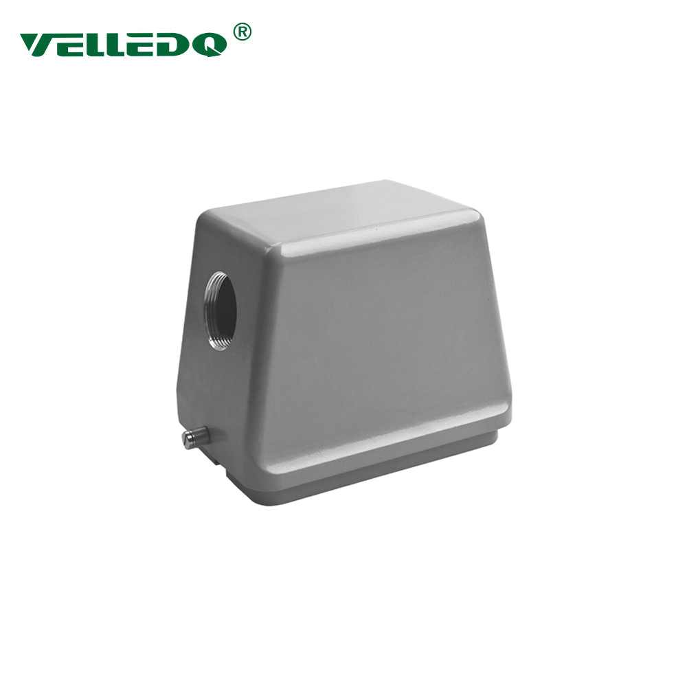

For many years, the semiconductor sector has led the way in technical innovation, which has fueled the global digital revolution. Semiconductors are the fundamental components of contemporary technology, appearing in everything from the tiny chips in our cellphones to the sophisticated sensors used in a plethora of applications and the intricate processors powering our computers. However, the creation and manufacture of these complex components depend on the semiconductor fabrication process, a highly specialized and complex manufacturing method. Creating integrated circuits (ICs) and other semiconductor devices is the intricate process known as semiconductor fabrication, often known as semiconductor manufacturing or semiconductor lithography. To meet the needs of a constantly changing digital ecosystem, this method has undergone continuous evolution. Integration of metal electric socket, which are essential to enhancing the effectiveness, dependability, and security of semiconductor production, is one of the most important aspects of this progression.
Semiconductor Manufacturing: A Chronological Review
Since its inception in the middle of the 20th century, semiconductor production has grown to become a vital component of contemporary technology. Creating electronic devices on a semiconductor substrate—typically silicon—is the process’s goal. The process is mainly divided into three stages: packaging, wafer fabrication, and design.
Design: The design stage is the first step in the manufacture of semiconductors. Using cutting-edge software, semiconductor designers and engineers may produce an intricate schematic of the electronic parts that will be etched into the silicon wafer. This is an important stage since it sets the final semiconductor device’s performance and functioning.
Wafer Fabrication: The process of fabricating semiconductor wafers starts as soon as the design is finished. This phase involves a number of intricate procedures, including as etching, ion implantation, photolithography, and more. Specifically, photolithography is essential because it makes it possible to precisely copy the design onto the silicon wafer using a number of mask layers.
Packaging: The semiconductor devices must be tested, segregated, and packaged into discrete components once they are produced on the wafer. Packaging is an essential stage because it offers the electrical connections required for integration into electronic devices while safeguarding the fragile semiconductor chips.

The Development of Manufacturing Semiconductors
There have been significant developments in the semiconductor manufacturing business since its start. Early semiconductor devices had a lot of features, were expensive, and were big. On the other hand, substantial advancements in manufacturing methods and machinery have resulted from the ongoing drive for miniaturization and performance enhancement.
Moore’s Law: The renowned prediction made in 1965 by Gordon Moore, co-founder of Intel Corporation, states that a semiconductor chip’s transistor count would double about every two years, increasing computer capability in tandem. Moore’s Law, a forecast that has remained true for decades, has propelled the unrelenting innovation in semiconductor production.
Cleanroom Technology: The environment used to manufacture semiconductors is among the cleanest in the world, necessitating tight control of pollution and airborne particles. Ensuring the quality and dependability of semiconductor devices has been made possible in large part by the development of cleanroom technology.
Advanced Lithography: The accuracy and resolution of photolithography, a crucial step in the creation of semiconductors, have been continuously improved. Extreme ultraviolet (EUV) lithography, which replaced ultraviolet (UV) lithography, has enabled producers to produce more complex and smaller semiconductor features.
Automation and robots: To increase productivity, reduce human error, and improve the overall quality of semiconductor products, automation and robots have been included into semiconductor production facilities.
Advanced Materials: Smaller, quicker, and more power-efficient semiconductor devices have been made possible by the development of novel materials like strained silicon and high-k dielectrics.
Case Study: EUV Lithography Machines Made by ASML
Let’s look at a particular example to show how metal electric socket affect semiconductor fabrication: the extreme ultraviolet (EUV) lithography equipment made by ASML. Using very small light wavelengths, EUV lithography is a state-of-the-art method for fabricating semiconductors that utilises complex patterns on silicon wafers. metal electric socket are essential to ASML’s state-of-the-art EUV lithography equipment for a number of reasons.
High accuracy: With features as tiny as a few nanometers, EUV lithography demands a very high level of accuracy. Metal electric socket help to improve lithography precision by supplying a steady and accurate power supply to the machine’s sensitive parts.
Cleanroom Environment: Extremely hygienic and regulated conditions are required in semiconductor cleanrooms. Metal electric socket are made with a low chance of contamination in mind, so the lithography process isn’t hampered by dirt or debris.
Reliability: The EUV lithography machines made by ASML are sophisticated, high-priced devices. Metal electric socket minimize the possibility of expensive maintenance and downtime by guaranteeing the dependability and uptime of these devices.
Problems in the Fabrication of Semiconductors

Metal electric socket have significantly enhanced the process of fabricating semiconductors, however there are still some difficulties involved.
Miniaturization: As semiconductor devices become increasingly compact and intricate, there is an increasing need for manufacturing techniques to be even more precise. Metal electric socket are faced with a difficulty because of this: they must continue to be durable and reliable while adjusting to ever-smaller dimensions.
Environmental Concerns: Like many other industries, the semiconductor sector is becoming more conscious of its environmental impact. As a result, the demand to provide ecologically friendly connections and manufacturing techniques is increasing. This entails cutting down on energy use and using less dangerous materials while making connectors.
interruptions to the Supply Chain: The semiconductor sector has seen supply chain interruptions recently, which have affected the accessibility of essential components. Metal electric socket are no different, and in order to satisfy the needs of semiconductor production facilities, manufacturers must have a steady supply chain.
Data Security: As data transfer becomes more crucial in the manufacture of semiconductors, protecting data becomes of utmost significance. In addition to transmitting data quickly, connectors also need to shield it from online dangers.
Prospects for Semiconductor Manufacturing in the Future
A number of fascinating advancements and trends in semiconductor manufacturing are anticipated as the field continues to grow:
Nanotechnology: To push the boundaries of miniaturization, the semiconductor industry is aggressively investigating nanoscale manufacturing processes. This will need the development of connections that can handle nanoscale characteristics, but it may also lead to the fabrication of ever smaller and more powerful electronics.
3D Integration: 3D integration is becoming more and more popular as a means of improving the performance and efficiency of semiconductor devices. This method involves stacking semiconductor components in many layers. Enabling the vertical connections needed for 3D integration will be made possible by metal electric socket.
Materials Innovation: Scientists are always looking into novel materials, including graphene and carbon nanotubes, for the production of semiconductors. Although these materials have special qualities that have the potential to change the industry, they also present difficulties for connection compatibility and design.
Integration of Artificial Intelligence (AI): AI and machine learning are becoming more common in semiconductor manufacturing, enhancing process optimization and control. AI-driven systems will need metal electric socket to meet their high-speed data transmission and power needs.
Initiatives for Sustainability: The semiconductor sector is moving in the right direction. This involves creating connections that have a less environmental effect and figuring out how to recycle and reuse the resources used to make semiconductors.
Quantum computing: Although it is still in its early stages, this technology has the potential to completely transform computer capability. The particular connections needed by quantum computers, which operate at very low temperatures, will need metal electric socket to adapt to their unique needs.
In summary
The constant quest for more compact, quick, and potent semiconductor devices has resulted in significant changes to the semiconductor industry since its founding. All along this trip, the production of semiconductors has been essential to the evolution of technology.
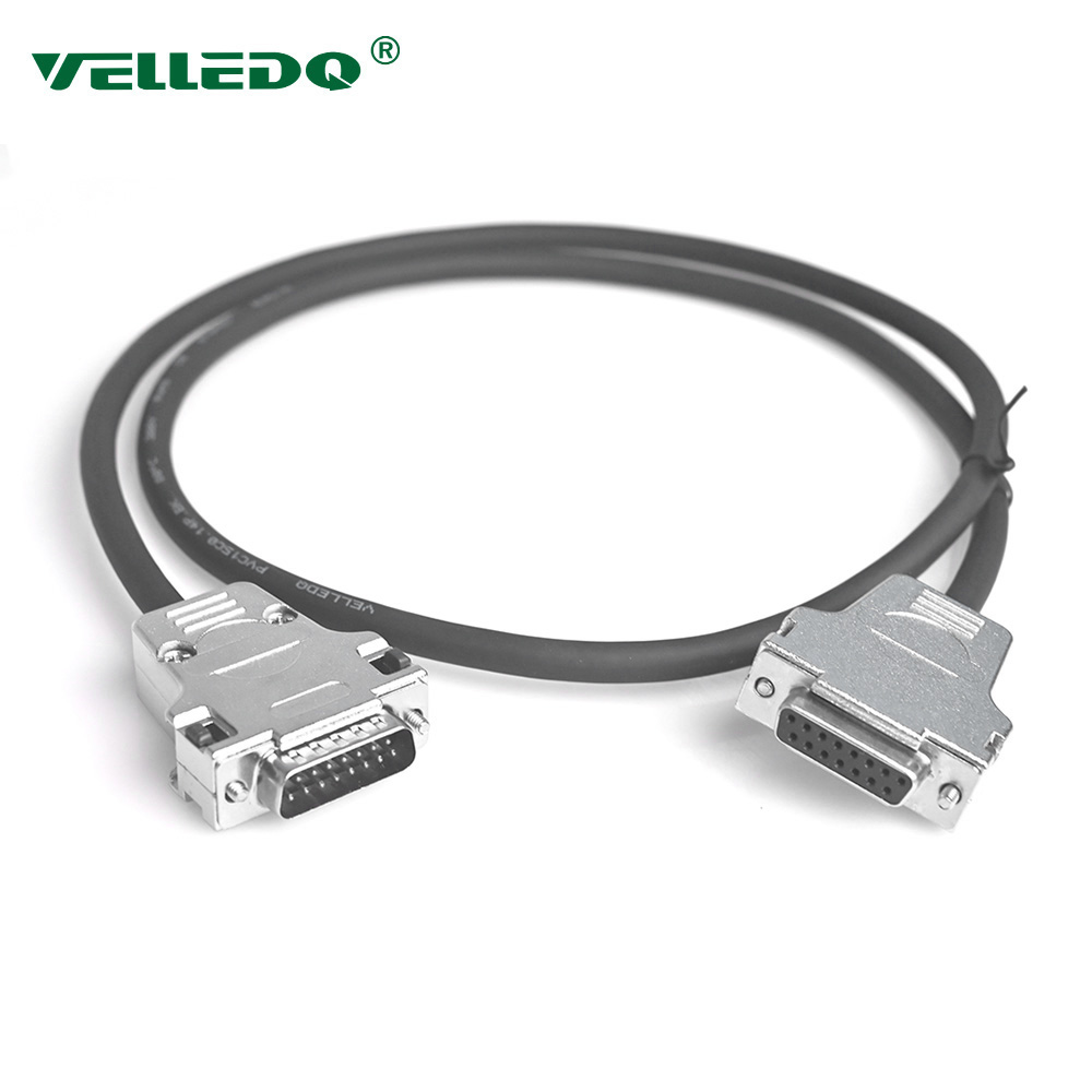
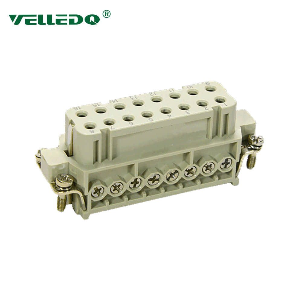
Metal electric socket have become an essential part of the semiconductor production process, improving efficiency, safety, and dependability in cleanroom settings. The future generation of semiconductor devices depends on the development of cutting-edge technologies like EUV lithography equipment, which have been made possible by these specific connections.
Metal electric socket will undoubtedly continue to be a pillar of semiconductor manufacturing as the semiconductor business pushes the envelope of innovation, guaranteeing the dependable creation of the electronic components that run our contemporary world.